Abstract
Designing a printed circuit board.
For this week’s assignment, I decided to start thinking about the circuitry of my theremin and to come up with a first model for it. This is very likely a first iteration and far from the final product.
After chatting with Anthony during the first review, he gave me a few starting points for my final project. As I was anticipating, I will have to wait for the input and output devices weeks to correctly design a fully working board, but I decided to give it a shot already this week. To that end, I decided to combine on a single board the functionality of two step response detectors (see input devices) with that of an MP3 player with a speaker (see output devices). Here are the design choices I made for the circuit, even though they may not necessarily be the correct ones yet:
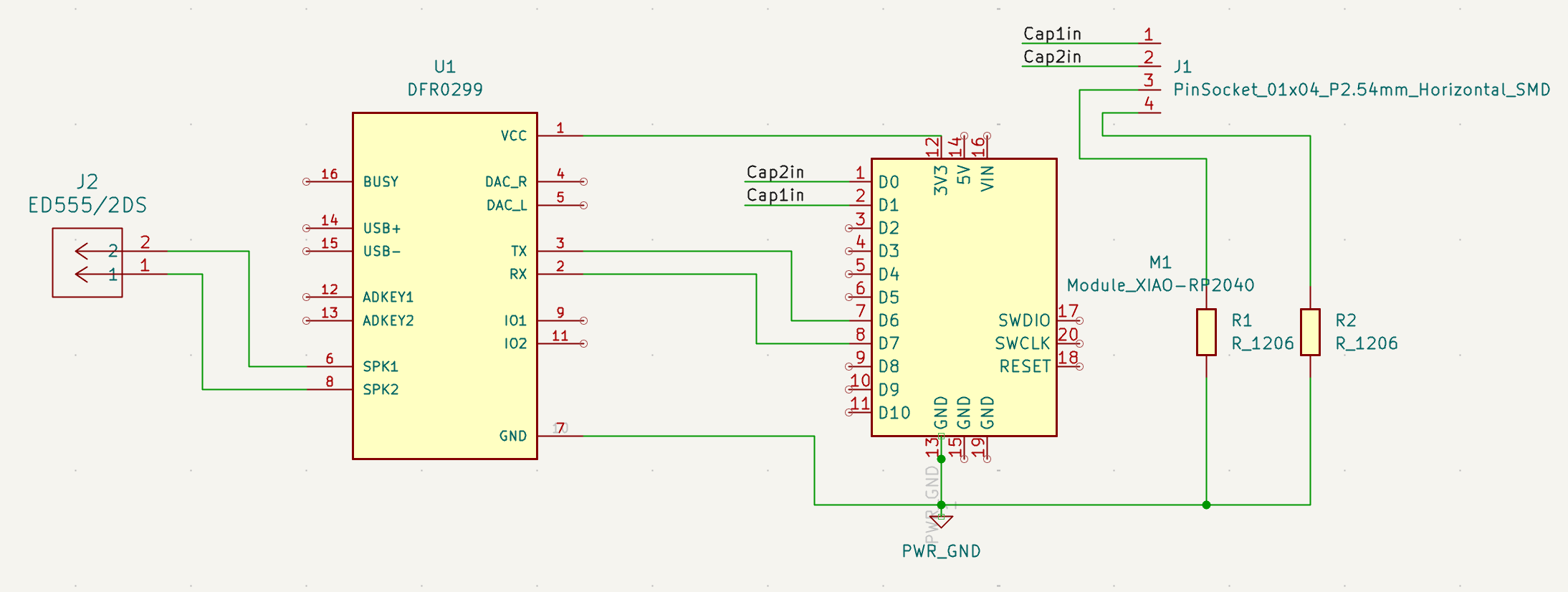
- I decided to base the board on an RP2040 microcontroller embedded in a XIAO module. It seemed like this choice constrained me to use pull-down resistors connecting the capacitive detectors to ground, as the RP2040 doesn’t have a built-in QTouch/FreeTouch protocol, unlike other microcontrollers like the SAMD21. It may turn out later that a different microcontroller could be the better one.
- I decided to use the MP3 player module DFR0299 with the ED555/2DS speaker. The more I think about it, I believe that an MP3 player isn’t the most suited technology to synthesize sounds from their pitches based on the inputs to the microcontroller.
- I decided to have the two capacitive input devices be external to the board (as would be the antennae on a real theremin). For that, I connected the two detection ports, as well as two connections to ground through a pull-down resistor, to a 4-pin header, which I would then connect to the input antennae.
- I decided to use the D0 and D1 GPIO pins of the XIAO for the input devices as their other dedicated function is analog input. The MP3 module uses the UART protocol so its connections had to be through D6 and D7 (as well as ground and supply voltage).
With these choices in mind, the schematic below shows a possible circuit. Interestingly enough, I couldn’t find the symbols and footprints for the speaker and MP3 module in the Fab Kicad library so I used those downloaded from the manufacturers directly.
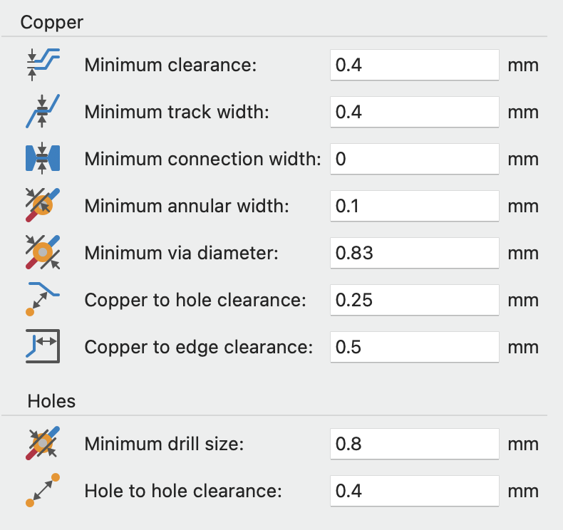
After this, I switched to laying out the footprints on the actual PCB. First, I set up the design rules for the EECS PCB milling machine.
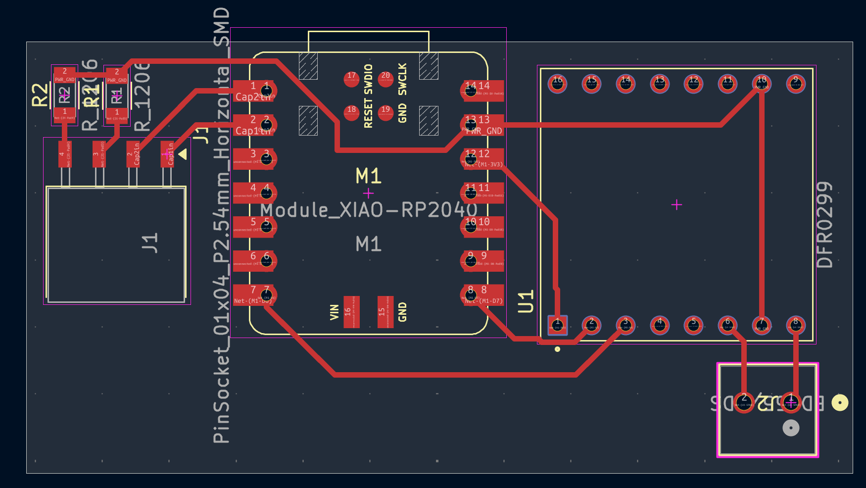
Then, I proceeded to untangle the components and lay them out with tracks on the board. This took a bit of playing around (due to having 6 footprints to consider), but after some rotations and flips, everything laid out nicely on a single layer on the board. I am not sure if the current position of the four pin header is functional, but it should be easy to just move it lower on the board if it needs to be next to the board edge.
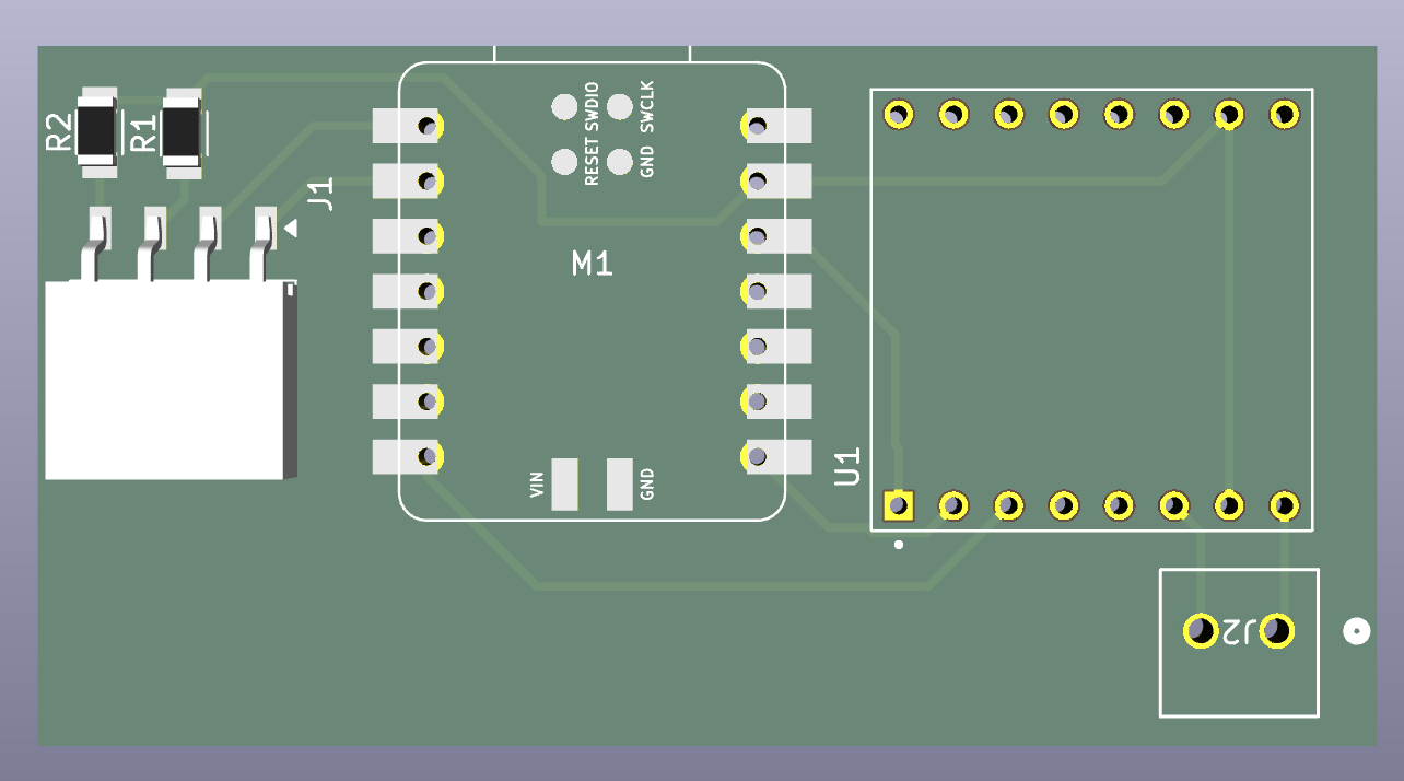
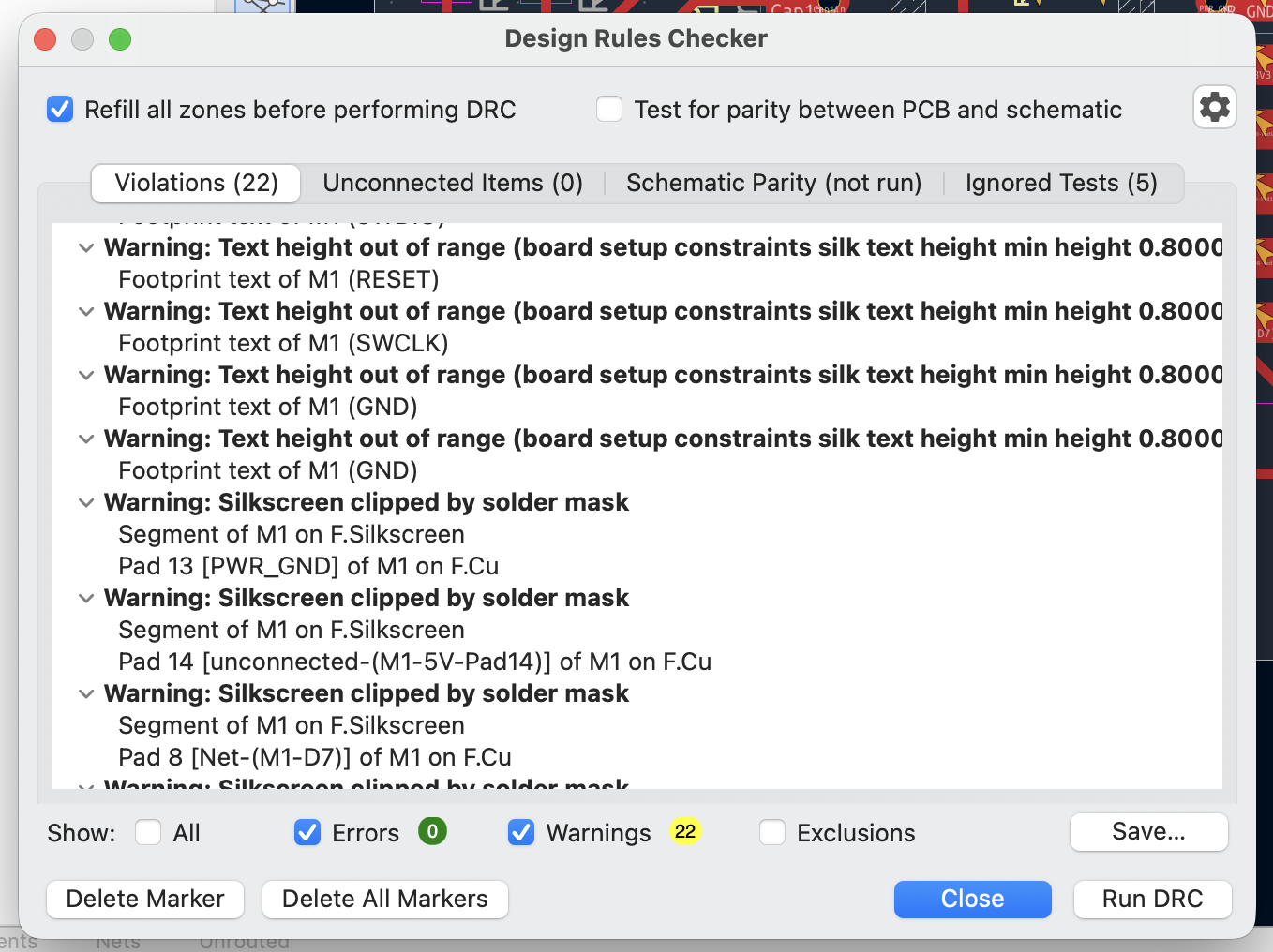
Finally, my board passed the Design Rule Check, with only a couple of aesthetic warnings!