
A contact input board
This board connects two contact switches to a Seeed XIAO RP2040. It is a small first step toward the contact-aware mobile robot proposal: read left and right contact independently, report the state over USB, and light a status LED when either input is active.
The XIAO provides the microcontroller, flash, clock, USB and voltage regulation. The new carrier adds the input circuits, an external LED, power and signal test points, and solder pads for external switches and two spare GPIOs. It uses USB power and 3.3 V signals.
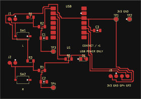
From switch contact to a digital input
Each normally open switch pulls a RAW node to ground. A 10 kΩ resistor holds that node high when the switch is open. A 1 kΩ series resistor and 100 nF capacitor filter the signal before it reaches the GPIO. The external switch pads are parallel to the onboard buttons.
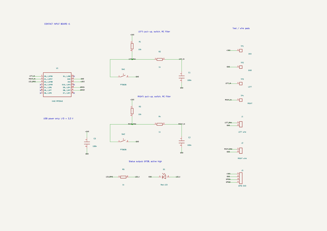
| Function | XIAO / RP2040 pin | Connection |
|---|---|---|
| Left contact | D0 / GPIO26 | Filtered input, TP3; J1 accepts a passive external switch. |
| Right contact | D1 / GPIO27 | Filtered input, TP4; J2 accepts a passive external switch. |
| Status LED | D2 / GPIO28 | Active high, 1 kΩ series resistor, red 1206 LED. |
| Expansion / scope | D9 / GPIO4; D8 / GPIO2 | J3: 3V3, GND, GPIO4, GPIO2 from left to right. |
| Power | USB; 3V3 and GND | TP1 / TP2, plus an additional 100 nF bypass capacitor. |
The nominal release time constant is (10 kΩ + 1 kΩ) × 100 nF = 1.1 ms. During a press, the low-resistance switch makes the discharge time constant approximately 0.1 ms. The diagnostic firmware adds a separate 10 ms stable-input check because RC filtering alone does not establish complete switch debounce.
The RP2040 specifies a low input at or below 0.8 V and a high input at or above 2.0 V with 3.3 V I/O power. Those limits provide a way to compare the analogue input waveform with the digital result. See the RP2040 datasheet, GPIO DC specifications.
Layout and fabrication checks
The first single-layer routing attempt left the common ground connections obstructed. The final r1 layout uses two copper layers: components and signals on the front, a ground plane on the back, and eleven plated through vias connecting the ground pads to that plane.
Back copper layer
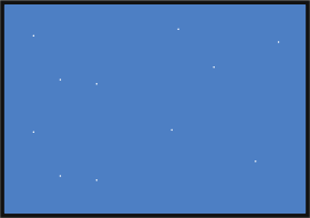
The design rules use 0.4 mm minimum track width, 0.4 mm copper clearance and 0.5 mm copper-to-edge clearance. The vias have 0.8 mm copper diameter and 0.4 mm drill diameter. KiCad 7.0.11 reported:
0 DRC violations
0 unconnected pads
0 footprint errors
An additional comparison checked the KiCad-exported schematic netlist against the PCB: 41 connected pads across ten functional nets, seven intentional no-connect pins, and all nineteen footprint assignments matched. This comparison supplements PCB DRC; native schematic ERC was not run.
The fabrication package contains both copper layers, solder masks, front silkscreen, outline and Excellon drills. It needs a process that supports two layers and plated vias. It is not ready for single-sided milling; the EDS fabrication route and local component stock still need confirmation.
Simulating a bouncing contact
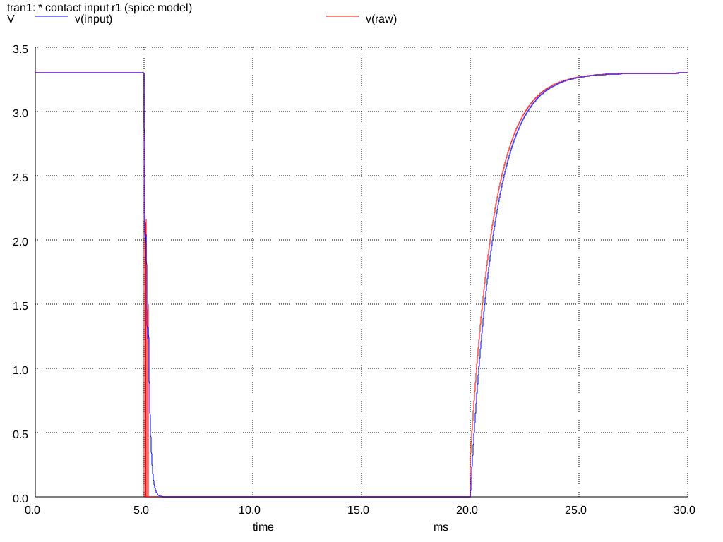
ngspice 42 simulated one input with the nominal resistors and capacitor, a fixed 3.3 V supply, and an ideal switch with 1 Ω on resistance. The input includes three short contact changes starting at 5 ms and a final release at 20.001 ms.
Inspect the simulated bounce
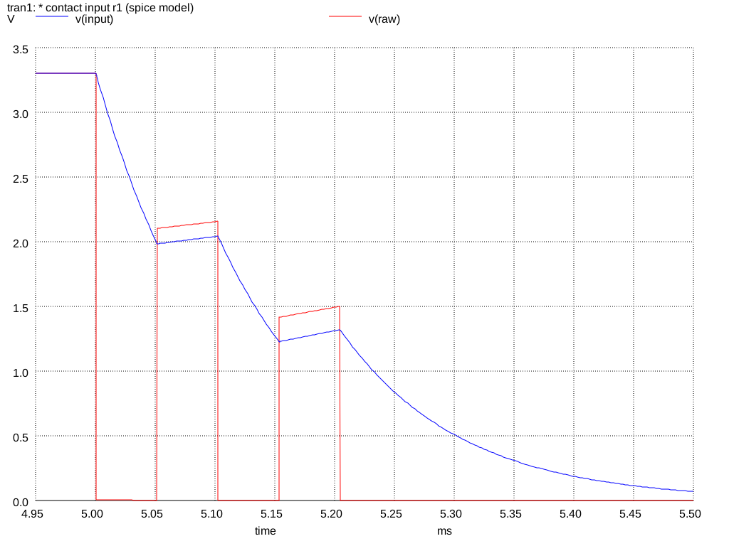
The simulated input is 3.300000 V while idle, 0.000329967 V while pressed, and 3.299077 V at 29 ms after release. It first crosses below 0.8 V at 5.254749 ms and reaches 2.0 V at 21.02516 ms, about 1.024 ms after the final release.
The model checks nominal charge and discharge behavior. Component tolerance, cable noise, real contact bounce and the MCU input circuit remain to be measured.
A diagnostic program for the bench
The program reads both inputs, applies the 10 ms stable-state check, lights the external LED, and sends raw and debounced states as USB serial CSV. GPIO2 produces a nominal 1 kHz square wave for oscilloscope observation. Software timing and serial activity can affect that waveform, so its period and jitter are measurement questions.
Target: rp2040:rp2040:seeed_xiao_rp2040
Arduino CLI 1.5.1 / Arduino-Pico 6.1.1
Program storage: 54,920 bytes
Global variables: 8,928 bytes
This is a successful local compile. The program has not been uploaded to the new board. It uses a different pin assignment from the Week 03 QPAD firmware.
Group assignment: instrument observations
Bench measurements are pending. The prepared procedure uses a multimeter to check 3.3 V, a compensated 10× oscilloscope probe to observe GPIO2, and two channels to compare RAW and the filtered contact input. It records probe ratio, sampling, trigger, period, logic levels, bounce and filtering delay.
The measurement sheet has empty reading fields. Actual group participants, instrument settings, captured waveforms and individual contributions will be added after the lab session.
Source and fabrication files
Download the KiCad project, source, checks and fabrication package · BOM · Native DRC report · Netlist comparison · SPICE measurements · Firmware build output.
The components are listed in the Fab inventory. Module pin mapping and footprint dimensions follow Seeed's original XIAO RP2040 documentation; the board does not use the Plus variant. Standard footprints come from the KiCad Community libraries, with their license retained in the download. The circuit, project generators and diagnostic source were prepared with Codex assistance.