This week, I will be designing an embedded microcontroller system for my final project. I chose to use an ESP32-S3 module for my final project because of the large number of pinouts and the extensive libraries available to operate my peripheral devices and sensors.
The ESP32-S3 module requires a crystal oscillator, a small set of inductors, flash, and other components. To avoid adding this large modeling effort to my process, I will be using the ESP32-S3-WROOM-1 module, which has a built in antenna and the required components.
I have 6 actuators per module: 2 servos and 4 DC motors (each with encoders). The servos can be directly powered with 5V and controlled with a GPIO pin. The motors, however, need to be driven and read. My plan is to use an h-bridge to control each motor. The integrated circuit DRV8847 is a dual h-bridge motor drive. This IC is rated for 1A RMS per h-bridge, which is perfectly acceptable for my system. The DC motors I purchased are rated for a no-load current of 40mA, with a maximum stall current draw of 1.2A. Although, this is higher than the rated current draw, I do not expect the load to be high enough to pull the full 1.2A current draw. If this is not true and I do require the 1.2A, I will switch to the TB67H451AFNG motor driver, which has a maximum current output of 3.5A.
I plan on using an external 12V battery, and an external 12v-5v buck converter. Both the 12V and the 5V will be accessible to the PCB, which allows me to use an LDO converter to convert the 5V to 3.3V for the ESP32-S3. I plan on using the AZ1117IH, a low dropout linear regulator.
I will design this circuit in Kicad. To start out, I downloaded the class library linked here. Then, I added the components outlined above, mapping one of the Hbridge's IN pins to GPIO pins 0-3.
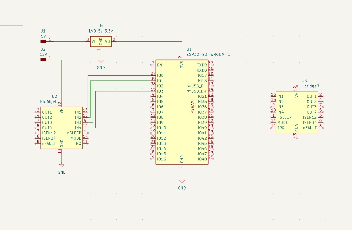
I added the wiring for the dual H-bridge, the LVO converter, and bypass capacitors, alongside connections for all of the motor's pins and the encoder pins. I grounded the ISEN pins because I have no interest in measuring current.
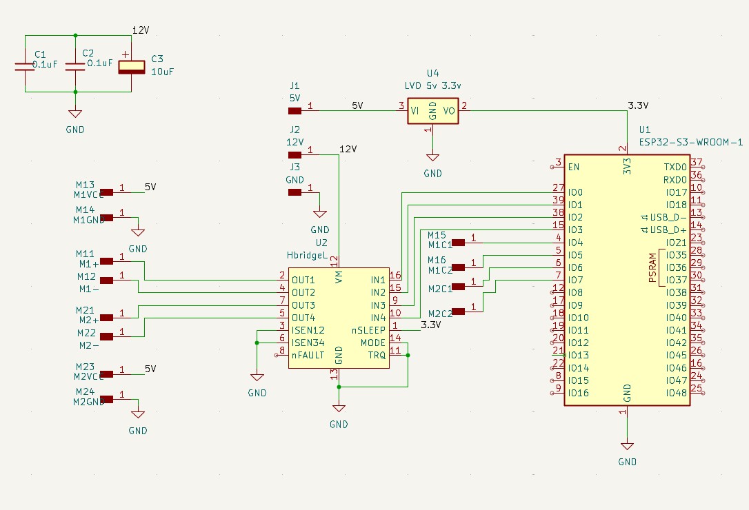
The wiring started to get ugly, so I resorted to using labels for most of my connections. Below is a series of modules, with labels connecting all of them. The input power has the +12V and the GND from my battery and 5V from my buck converter. I added bypass capacitors for all the voltages I operate at. I listed all the motor's input/output pins in the order they appear, added pins for my servos, and an LED to send status information
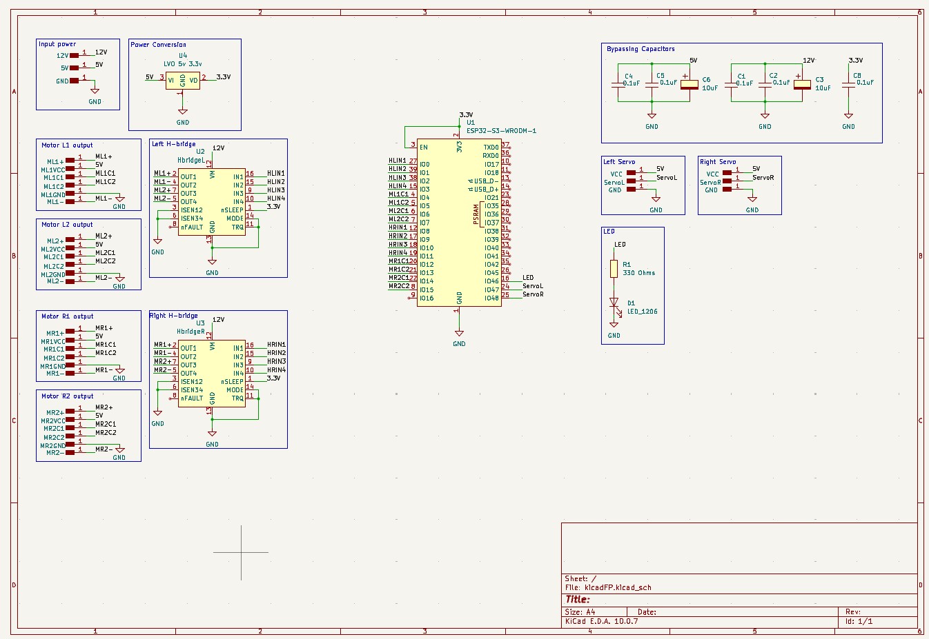
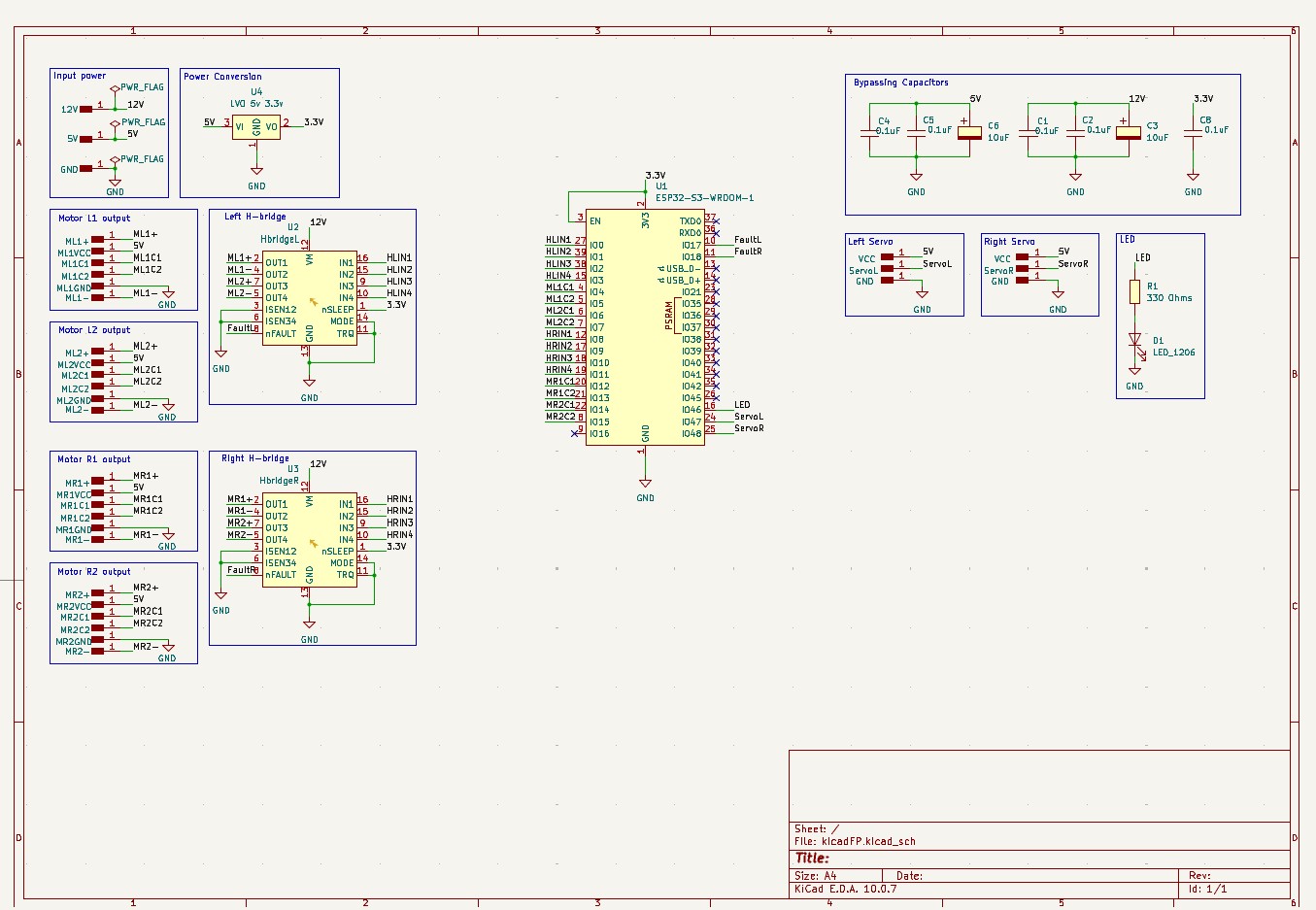
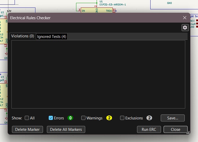
Now I was able to run ERC check, which gave plenty of errors. I had to mark all the unused pins as "Not connected", set a power flag on 12V, 5V, and GND, actually connect the nFault ins to the ESP32, and change the Hbridge's symbol (changed the ISENSE pins to passive, since the datasheet says it's OK to ground them if unused).
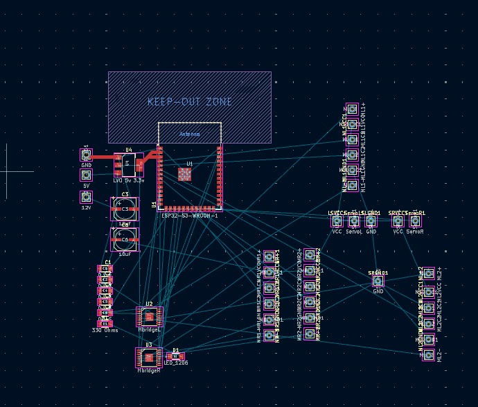
Now, I am able to work on the pcb layout, keeping in mind I can only manufacture boards with two layers. The image below shows what the parts look like before wiring them together. At the expense of what will be complicated wiring and traces, I would like to group pinouts together by the part they correspond to. In other words, I want all the motor 1 pins together, all the servo pins together, all the power pins together, and so forth.
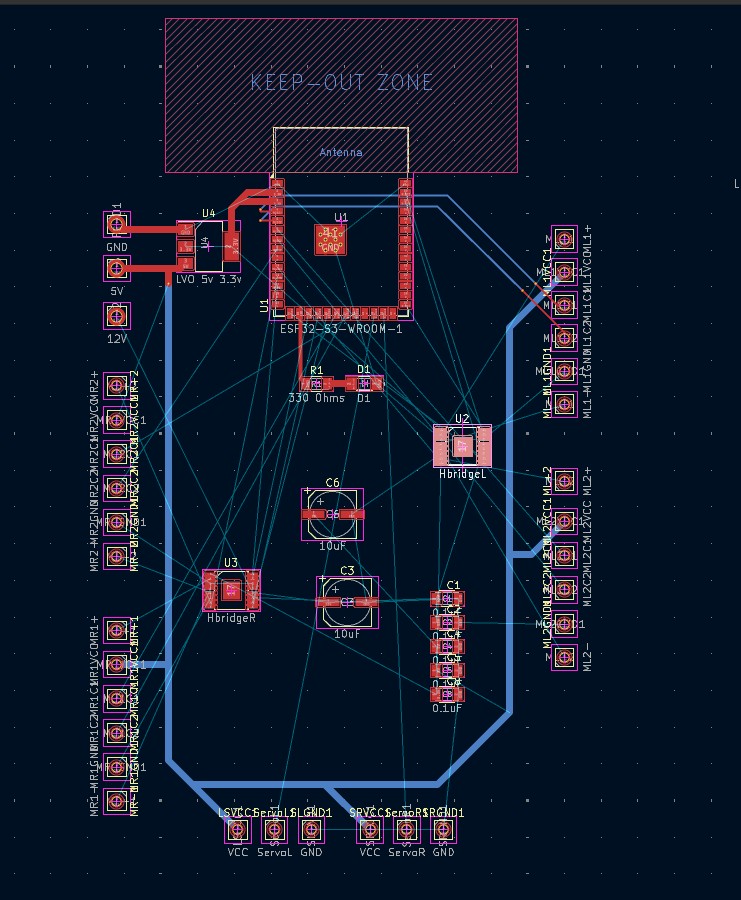
My initial attempts at wiring consisted of moving the power pins to the top left of the board and all the other pins along the sides of the pcb. The 5V that are necessary for the servos and motor encoder's VCC run around the board.
More wiring progress...
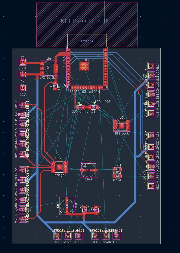
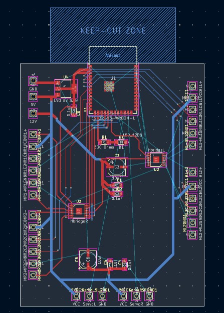
For this initial draft, I stuck to a principle of orthogonal wiring; wires on the front plate should generally go horizontally and wires on the back plate should go veertically. This worked pretty well and passed DRC, although I was still missing a lot of important details and parts.
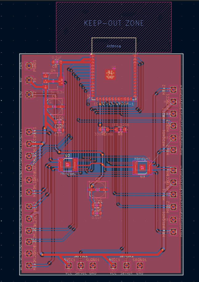
Firstly, I completely forgot about USB, so I added a basic microUSB pinout to the bottom of the board. I also forgot about switches. If I add a contact switch at the base of every joint with a DC motor, I can calibrate the motors on startup and control them based on absolute positioning, rather than relative. Lastly, the pcb needs to actually fit inside the main module, so the main cut needs to be under 3.5x3.5 inches.
Moreover, vias aren't as easy as I thought. Not only are the machines unable to make vias that small, but I need to manually sodder each one on both sides. This would be quite problematic and time consuming. Therefore, I increased the size of the vias, and veered away from my principle of orthogonal wiring to get away with the least number of vias possible. The final product has many, but it doesn't seem impossible.
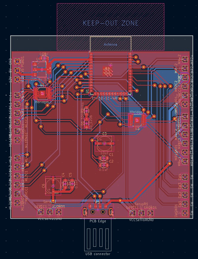
With that, I am ready to begin the milling process.